Near-infrared detection has important implications for applications such as spectroscopy, night surveillance, infrared guidance, and optical communications. In recent years, the development of CMOS technology has made Si-based optoelectronic devices widely used. Due to the large bandgap of Si, common Si-based photodetectors are generally unable to work effectively in the near-infrared spectral region beyond 1200 nm. In order to solve this problem, scientists deposited a thin metal film on the Si surface to form a Schottky junction between the metal and the semiconductor. The free electrons in the metal absorb the photon energy and pass through the Schottky barrier and enter the Si material. In the formation of photocurrent. The cutoff wavelength of this response is determined by the barrier height, thus breaking the semiconductor bandgap limitation. Under this photo-responsive mechanism relying on thermionic emission, the metal structure has a great influence on the near-infrared detection performance of the device. Currently, various metal nanostructures such as nanorods, nanowires, and gratings have been shown to enhance the heat based on, for example, transmission surface plasmon resonance (PSPR), localized surface plasmon resonance (LSPR), and resonator resonance. Electronic photoelectric response. However, the quantum efficiency of such structures is still low, and these finely-tuned nanostructures increase the complexity and production costs of the production process, making it impossible to realize large-scale, low-cost manufacturing. Recently, Chen Qilong, a professor at the Suzhou Institute of Nanotechnology and Nanobionics of the Chinese Academy of Sciences in collaboration with Southeast University Professor Wang Qilong, has made progress in the development of low-cost, high-efficiency silicon-based thermal electron infrared photodetectors. Researchers proposed a scheme for Au nanoparticle-modified Si pyramid structures. Experiments have shown that the properties of these devices can be comparable to those of well-designed and costly Si-based near-infrared photodetectors, and are expected to be applied to large-scale thermo-photovoltaic cells. And low-cost infrared detection. Related research results were published on Nanotechnology. The process adopted by the researchers is very simple. The use of standard anisotropic chemical wet etching methods to achieve the construction of Si-based pyramids; a layer of Au film is sputtered on the surface; and modified gold nanoparticles are formed by rapid thermal annealing; On the pyramid side, an ITO thin film was deposited by magnetron sputtering and an aluminum film was deposited on the other side by thermal evaporation as a back electrode; the sample was welded to the chip carrier by indium tin to complete the fabrication of the detector (Figs. 1 and 2). They found that the pyramid surface enhanced the coupling effect between incident photons and Au nanoparticles because the pyramidal surface reduced the back-reflected light and caused the photons to be multiplely reflected inside the Au nanoparticle, increasing the distance the incident light traveled. Au nanoparticles The introduction of the device also enhances the local electromagnetic field of the device, so that photons can be significantly absorbed and the photoelectric conversion quantum efficiency is improved. The researchers used the Au nanoparticle-medium-gold mirror structure to make full use of the wide-band high optical absorption of disordered metal nanoparticles and the omnidirectional Schottky junction composed of Au/TiO2/Si in both optics and electricity. At the same time, improve the internal and external quantum efficiency of photoelectric conversion. This dense hot spot distribution enhances the efficiency of light absorption and thermionic emission. The photoresponsivity is one of the highest results at present, and the silicon photoelectric response cut-off wavelength has been extended to nearly 2 um, demonstrating an effective near-infrared silicon base. Optoelectronic applications. In addition, through the time-resolved IV forward and reverse bias test analysis, they analyzed the relationship between the thermal electron photoelectric effect and the photothermal effect in the photo-thermoelectric process, and uncovered the photothermal effect of the parasite's parasitic light emission process neglected in previous work. The enhanced thermal electron emission of surface plasmons provides important basis and reference for photoelectric conversion, photocatalysis, and light sensing applications. Related results were published on Laser & Photonics Reviews. This work was supported by the National Natural Science Foundation of China and the Chinese Academy of Sciences. manual ignition valve,manual ignition,manual ignition device GUOLONG PRECISION VALVE CO.,LTD , https://www.glstovevalve.com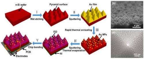
Fig.1 Schematic and experimental results of the manufacturing process of Si pyramid decorated with Au nanoparticles 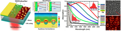
Fig.2 Silicon-based thermionic photodetector with Au nanoparticle-medium-gold mirror structure, band structure, optical characterization and experimental SEM image 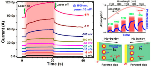
Figure 3 Photoelectric test analysis results