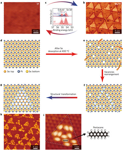
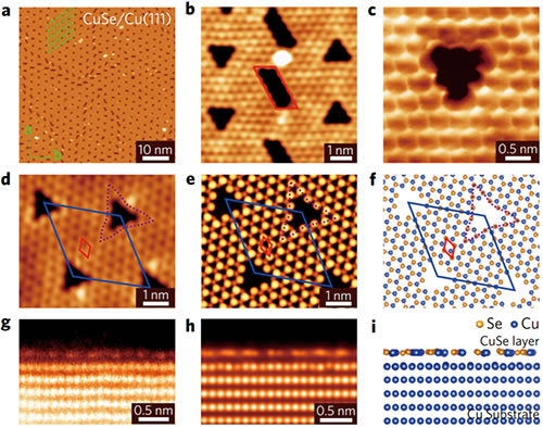
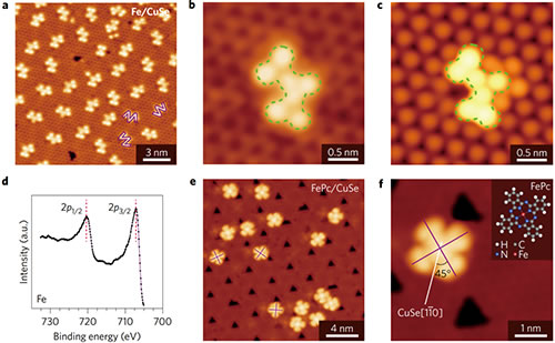
Figure 1 1H/1T patterned monolayer PtSe2 film. a: Schematic representation of triangular patterned 1T/1H-PtSe2. b: STM image of 1H/1T-PtSe2 film. Ce: STM images of 1H/1T-PtSe2 domains of different sizes. Fh: High-resolution STM images of 1H-PtSe2 domains (f), 1H-PtSe2 and 1T-PtSe2 interfaces (g), and 1T-PtSe2 domains (h). Ik: STM simulation images of 1H-PtSe2 domains (i), 1H-PtSe2 and 1T-PtSe2 interfaces (j) and 1T-PtSe2 domains (k). Figure 2 Reversible and molecularly selective adsorption of 1H/1T-PtSe2 films. a,b: STM images of 1T-PtSe2 (a) and 1H/1T-PtSe2 (b). c: XPS line of the reversible transformation process. Dg: Schematic diagram of the transition from 1T-PtSe2 to 1H/1T-PtSe2. h: STM image of pentacene molecule selectively adsorbed in 1H-PtSe2 domain. i: High resolution STM images of pentacene selective adsorption. Figure 3 Single layer CuSe structure with periodic hole pattern. a: STM image of a single layer of CuSe patterned in a large area, and the green lattice in the figure indicates the pore structure with a period of 3 nm. b: STM image of a single CuSe domain boundary. c: High-resolution STM image of a single triangular hole. Df: High-resolution STM image (d) with periodic pore structure CuSe thin film, STM theoretical simulation image (e) and corresponding theoretical model (f). Gi: STEM image (g) of a single layer CuSe film cross-section, simulated STEM image (h) and corresponding structure (i). FIG. 4 shows the functional characteristics of periodic CuSe films. a: STM image of a single-layer CuSe film with a W-shaped Fe13Se7 cluster embedded in a triangular hole. b: High-resolution STM image of a single W-shaped cluster. c: Single W-cluster STM simulated image. d: XPS spectrum of Fe element in Fe13Se7/CuSe. e: STM images adsorbed on CuSe films were selected by FePc molecules. f: High-resolution STM images of single FePc molecules adsorbed on CuSe surfaces. Graphene is a honeycomb monolayer composed of carbon atoms. In 2004, Andre Geim and Konstantin Novoselov succeeded in preparing graphene using exfoliation methods and discovered their novel quantum properties. They thus won the 2010 Nobel Prize in physics. Graphene has excellent properties such as high carrier mobility, ultra-high light transmittance, quantum Hall effect at room temperature, and so on. It has tremendous potential in the fields of electronics, optics, magnetism, catalysis, energy storage, and sensors. The application prospects, known as "future materials" or "transformative materials," have triggered a worldwide boom in the exploration and research of new two-dimensional crystal materials. In recent years, the research team led by the academician of the Institute of Physics of the Chinese Academy of Sciences and the academician of the Institute of Physics of the University of Chinese Academy of Sciences Gao Hongji conducted research on the preparation, properties, and applications of graphene and graphene-like two-dimensional atomic crystal materials. Habitat international frontier research results. Over the past ten years, they have used molecular beam epitaxial growth to prepare large-area, high-quality graphene and 2-D graphene-like atomic crystal materials, such as: graphene, silylene, decene, pinene, and diselenide. Platinum and terpene, etc. Most of these material systems were first created in the world and they have taken the lead in the international market. The successful construction of these new two-dimensional atomic crystal materials not only enriched the two-dimensional atomic crystal material library, but also laid the foundation for exploring its physical properties and potential applications. In general, two-dimensional atomic crystal materials need to be functionalized or patterned before they can be used for further applications. For example, in the semiconductor industry, semiconductor materials need to be first patterned using photolithography, followed by electron doping or hole doping to form PN junctions and transistors. The functionalization of a two-dimensional atomic crystal material can be achieved in various ways, for example by depositing molecules or atoms onto the surface of a two-dimensional atomic crystal material, or introducing another two-dimensional atomic crystal material to construct a laminated structure. Recently, the joint research team led by Gao Hongyi has made breakthroughs in the research of new two-dimensional atomic crystal materials and their functionalization. They studied two kinds of chalcogenide-based two-dimensional atomic crystal materials and constructed for the first time two “nano-scale natural patterns†materials: one is a 1H/1T monolayer of selenium with alternating triangular puzzle patterns. Platinum (1H/1T-PtSe2), the other is a single layer of copper selenide (CuSe) with periodically arranged triangular holes. Further experiments on the deposition of molecules and atoms on the surfaces of these two materials revealed that these two kinds of two-dimensional atomic crystal materials are selectively functionalized. Monolayer PtSe2 has two configurations, octahedral (1T) and triangular prismatic (1H). Prior to this work, in 2015, the research group prepared a 1T monolayered platinum-selenide (1T-PtSe2) single crystal thin film with high quality semiconductor properties using a direct selenization Pt(111) substrate method. Based on this work, they anneal 1T-PtSe2 to form selenium vacancy defects on the surface. The vacancy defects are rearranged to obtain a triangular patterned 1H/1T-PtSe2 monolayer film. By further adding selenium to the film and annealing at a lower temperature, a pure 1T-PtSe2 film can be obtained, thereby achieving a reversible transition between the 1H/1T-PtSe2 film and the 1T-PtSe2 film. In order to verify the potential functional properties of the material, they deposited pentacene molecules onto the 1H/1T-PtSe2 surface and found that the pentacene molecules selectively adsorbed in the triangular 1H-PtSe2 region. In a further experiment, they deposited selenium atoms on the surface of a Cu(111) single crystal. For the first time, they successfully constructed a novel graphene-based two-dimensional atomic crystal material CuSe. The single-layered CuSe has a honeycomb structure. The selenium atoms and the copper atoms in the six-membered ring are alternately arranged to form a novel two-component two-dimensional atomic crystal material. At the same time, in order to release the stress due to the lattice mismatch of CuSe and Cu(111) A single layer of copper selenide forms a hexagonal arrangement of periodic nanohole structures, forming a natural patterned two-dimensional atomic crystal material. The shape of the hole is an equilateral triangle with a side length of 1 nm. According to the calculation of the density functional theory, only three neighboring CuSe six-membered rings are periodically deleted and the CuSe and Cu can be completely released (111) due to a lattice mismatch. The resulting stresses form a periodic array of triangular holes. They deposited iron atoms and iron phthalocyanine molecules (FePc) onto a single layer of copper selenide. It was found that iron atoms only formed Fe13Se7 clusters inside the triangular holes, while FePc molecules selectively adsorbed in non-porous areas. It is worth mentioning that 1H/1T-PtSe2 and CuSe, two kinds of new two-dimensional atomic crystal materials with nanoscale natural patterns, although they are obtained in an ultra-high vacuum environment, are also very stable in the air. Potential applications for functionalization of both materials. Related work was published in Nature Materials (10.1038/nmat4915, 2017). Joseph W. Lyding, an internationally renowned scholar and professor at the University of Illinois at the same time in the journal "News and Perspectives", titled "Chalcogen-based two-dimensional materials - nanoscale natural patterns" as the title, giving this work a high degree of The evaluation pointed out that "in the preparation of PtSe2 and CuSe monolayer structures, a method for constructing nanoscale precise regular patterns was developed", "if the method of natural patterning confirmed by Gao Hongyi and his team members is extended to a large class of chalcogenide Compound-based two-dimensional materials will create more opportunities for the preparation of nanoscale devices and chemical process systems." The work was funded by the Ministry of Science and Technology, the National Natural Science Foundation of China and the Chinese Academy of Sciences. Working Light,Led Work Light ,Magnetic Work Light,Car/Truck Work Light Lamp NINGBO ZHENGUO INTELLINGENT LIGHTING CO.,LTD , https://www.nbzguolight.com